DFM (Design For Manufacture) was once an after thought of the design process or a value added service carried out by EMS (Electronic Manufacturing Service) partners.
Manufacturing partners and design engineers now strive to collaborate on DFM much earlier in the design process, this benefits both parties and can often reduce time to market and improve production speed. With the 10 points below you can take the next step on the DFM learning path of improving your DFM and your relationship with your EMS partner without increasing your workload or extending your project timeline.
The easiest way to improve your DFM is to collaborate with your manufacturing partners!
Coherent work instructions
When outsourcing any manufacturing process it is vitally important that your build instructions are interpreted the correct way. These additional instructions may be for conformal coating, BGA/CSP underfill, component standoffs or other design specific requirements. As technology moves on, processes get more complicated, so it is imperative to have the best instructions possible. If you design it right anyone can build it!
Useful data formats
Data formats are a major factor that PCB professionals have been collaborating on over the past 10 years, the main talking point has always been finding a useable replacement for Gerber files. The creation of OBD++ files could have completely taken over as an all in one production pack, however, a lot of engineers in both design and manufacturing trust and understand Gerber files with a separate BOM and P&P file.
Good PCB revision control
One issue with separate files for PCB drawings, schematics, BOM and P&P files is that you have a lot of different files to juggle and some changes may or may not impact them. It is imperative to have a solid doccument revision control system that is applied to all projects regardless of how small the change. Implementing this will improve more than just your DFM, it can streamline your whole product logistics flow.
Ensure no EOL (end of life) components
A key consideration in the very early stages of design is to ensure that all of your core components are not approaching end of life. This EOL check can be carried out by your manufacturing or kitting partner and is a great way for them to add value to their services. Finding EOL components during prototyping can cause a lot of pressure to get a quick redesign completed and could start the NPI process all over again!
Clear component reference and polarity on PCB/drawing
When creating a production program for advanced machinery time is of the essence, a clearly labelled PCB or drawing with component reference and polarity markings can ensure that production engineers make the right decision in a prompt and efficient manner. This means that your product is built on time and more importantly will be 100% correct first time, every time.
Minimise line items
One easy change to make for DFM is to standardise some of your passive components, it often proves more cost effective to have common passive components for example; having an 0402 100nF 25v and an 0402 100nF 10v on the same board in similar volumes it would be most cost effective to change to just 0402 100nF 25v in most cases.
Complete BOM with Alternatives and DNF list
One of the most important documents for any production partner is the BOM this will be the definitive source of information for all of the components to build your product. The BOM should include as a minimum; Component references – R1,R2,R3, Component description – 0402 10k 5% 0.125W, Component part number – 100RES0001, Manufacturers part number – CRG0402J10K/10, Alternative manufacturers part number if acceptable and a DNF(do not fit) list for parts not needed in this build specification.
Accurate PCB footprints or land patterns
As you start to build up your component library you may receive feedback from your EMS partner as a DFM report, this will usually include PCB footprints on your product that could cause reliability issues or cause the product to not meet the required IPC standard. These changes are a natural part of the NPI process and making them will yield a perfect product ready for volume production. Being extra strict with your component footprint library is essential, especially where multiple PCB design professionals are using the same library.
PCB panel rules
When PCBs are manufactured they are very rarely made as a single image or “1 up panel”, they are usually stepped up to fit as many on a sheet as possible. This makes the whole process more cost effective for both parties involved as your PCB manufacturer efficiently uses their materials and you as a customer get a more competitive price for your PCB manufacturing. After PCB manufacturing is finished it is time to assemble the PCB, the large sheets used in PCB manufacturing are usually broken down into smaller panels to be assembled. This could be a single circuit on a large PCB or any number of circuits to make the PCB around 300mm x 400mm in size. This will need to have breakout points around each circuit and an extra 10mm border for machine handling without damaging components in the extremities.
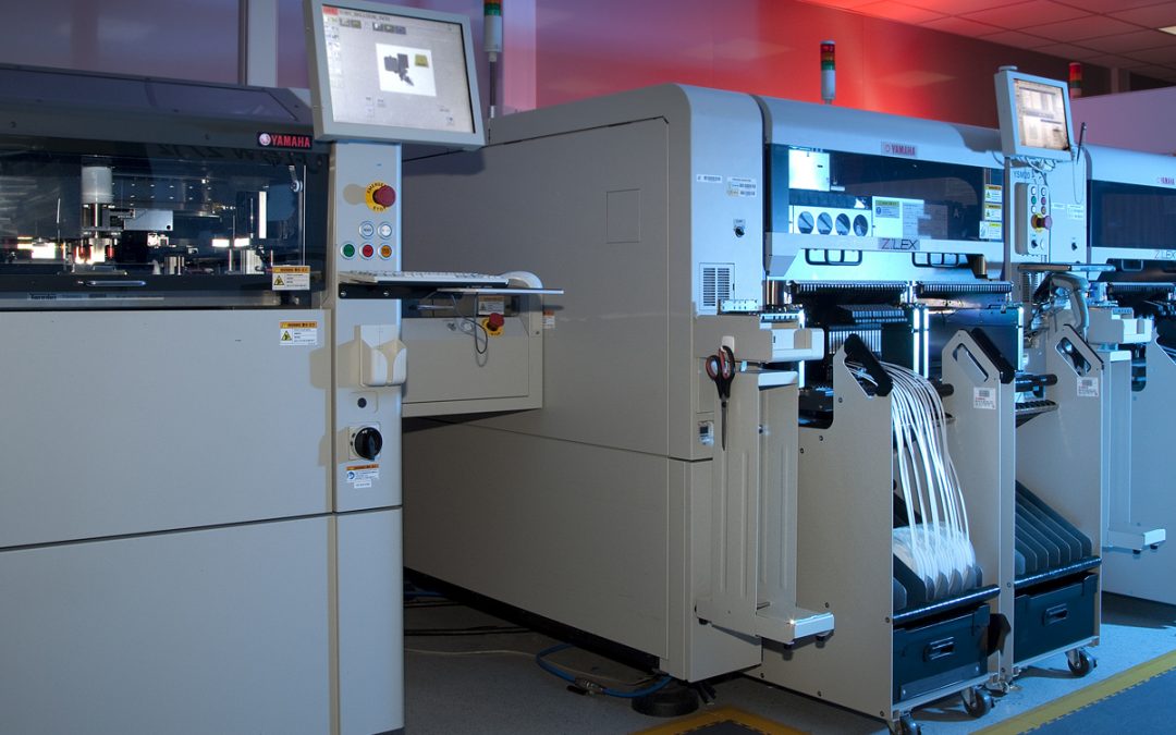
Complete Pick and place file
As well as generating a BOM and a Gerber set your EMS partner will also need a pick and place file in order to assemble your PCB with their high accuracy placement equipment. This file will designate which components will be placed in which position and should be directly linked to your BOM to ensure there are no discrepancies. A perfect P&P file will include the following information; Component Reference – R1, Component part number – 100RES0001, Component Description – R0402 10K 5% 0.125W, Manufacturers part number – CRG0402J10K/10, Mid point X(mm) – 10.254, Mid point Y(mm) – 22.500, Orientation angle – 270 and PCB side – Top.
The location, orientation and placement side information can be added to your BOM to make revision control easier for both parties and to simplify document handling.
